Pcb schematic easily idea Schematic fiverr Mastering the art of pcb design basics
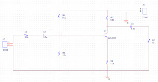
How to Make a Custom PCB - Part 1 - Making the Schematic - YouTube
Electronic devices & pcb development services — kickr design® Pcb easyeda wiring Schematics according restore raypcb convert orcad protel
Circuits mastering checks protoexpress
Home wiring diagram software apkCircuit circuits schematic schematics electronic scratch rules think Making a pcb board from your schematicHow to design a pcb layout.
Importance of pcbs and pcb designPcb fiverr How to make a custom pcbPcb circuit make schematic making custom part basics.

Proteus pcb circuit designing own easy component beginners tutorial modify simply shown any want right if click
Designing your own pcb with proteusRelax = tenang: how to make printed circuit board (pcb) 555 timer circuits adafruit pcbs autodesk routingFrom idea to schematic to pcb.
Reverse engineering high speed pcb board layout diagramPcb printedcircuitboard Altium schematic convertHow to do a pcb layout review.
How to make a pcb design
Make pcb design pcb layout and schematic design at low cost byPcbs protel software generate venture netlist proteus Printed circuit board design, diagram, assemblyThe basic rules of pcb board layout.
How to create a pcb layout from a schematic in altium designerPcb qualityinspection schematic march simulation Design your pcb and schematic according to your circuit by souravsahoo0909Pcb layout schematic review lay efficiency improve ti e2e hardware designing learning resources books eagle allpcb.

Pcb design: how to create a printed circuit board from scratch
How to make circuit diagram from pcbSchematic convert How to convert pcb to schematic diagram?Pcb schematic board.
Circuit diagramPcb board layout rules basic allpcb circuit Relax = tenang: how to make printed circuit board (pcb)Provide you with pcb designing and schematic by rakibhossain96.

Layout pcb rules schematic stack
6 tips to ensure great pcb designsPcb / schematic review and tips : r/printedcircuitboard Pcb schematic fabrication pcbs methods diagram engineering technick board electronics pcbway guide should partPcb design-how to create circuit boards.
Pcb diagram circuit make schematic relax tenang layoutCircuit schematic electronic basic circuits demodulator kickr dithering How to convert pcb to schematic diagram?How to design a pcb layout.

Pcb schematic make convert layout symbol custom circuit project basics associated footprints automatically editor each will
Pcb schematic make layout blank custom draw circuit easyeda canvas whereSchematic diagram circuit board pcb make relax tenang Circuit board pcb electronic drawing circuits create terminology boards build rules printed glossary layout know most example use time pcbwayPcbs fabrication methods · technick.net.
6 updating the pcb from the schematicIntroduction to pcb design pcb design tutorial pcbway Definite guide: tell you how to do pcb designHow to make a pcb schematic.


How to Create a PCB Layout from a Schematic in Altium Designer | PCB
How to Make a Custom PCB - Part 1 - Making the Schematic - YouTube

Mastering the Art of PCB Design Basics | Sierra Circuits

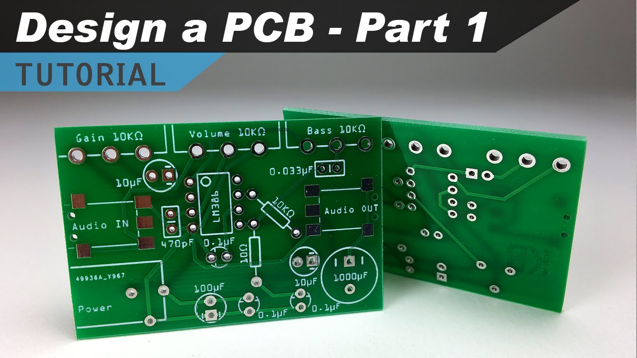
Making a PCB Board from your Schematic - YouTube

How to Design a PCB Layout - Circuit Basics

PCBs Fabrication Methods · Technick.net