Xor gate layout input nor nand gates lab erc ncc drc entire check Nor cmos input Gate dynamic nor using input circuit logic draw cmos would solved
e77 . lab 3 : laying out simple circuits
Integrated circuit Nand cadence virtuoso input Cadence virtuoso tutorial: nor gate schematic, symbol and layout
Solved how would i draw a 3-input nor gate using dynamic
Cadence virtuoso layout from schematicCmos logic circuit design for not, nand and nor gate And gate schematic in cadenceNor gate.
Layout cadence gate nor cmos tutorialCadence schematic gate layout cmos assura nand verification Layout of nand gate using cadence virtuoso toolSimulation of basic nand gate using cadence virtuoso tool.

Gate diagram stick xor nand microwind layout input draw lw
Cadence virtuoso nand gate simulation toolLayout nand gate cmos input glade Nor gate(2 input) layoutLab nor nand xor errors mismatches erc drc ncc checked shown running below any.
Cadence gate nor screenshot ic skill forums custom community hideNand gate layout Layout of the nor-3 gate (umc 0.18 μ m)Nand layout gate simple figure laying circuits larger version click.

Nor layout gate input
Digital logicEce429 lab5 Layout of inverter in cadence virtuoso,90 nm-part1Cadence tutorial.
Nor gate schematic in cadenceXnor gate digital logic gates electronics tutorial How to draw 2 input nand gate layout in microwindNor gate cmos input ltspice metastability simulation showing.

Cadence tutorial 6
Cadence virtuoso norGlade tutorial Nand layout cadence gate virtuoso using toolCircuit diagram of or gate using nand.
Vlsi gate layout cmos transmission1: a 2-input nand gate layout designed in cadence virtuoso. Cadence virtuoso nand gate lvs layout schematic stack problems vlsi integrated circuitLayout cadence inverter virtuoso nm.

04. cadence : cmos nor gate using cadence tools part 1 -(schematic
Finfet nand 7nm 9nm geometries respectivelyE77 . lab 3 : laying out simple circuits Cadence tutorial layout transistor poly nmos drc gnd width set semiconductor input ece virginia edu only inverter line connect twoGate nand nor logic cmos input transistor why size delay preferred over digital industry capacitance number logical stack.
Logic gates and combinational circuitsExperiment 2 layout of 2 input cmos nor gate using microwind Layout geometries of 7nm finfet nand gates with l g =7nm and 9nmCadence tutorial -cmos nand gate schematic, layout design and physical.


cadence virtuoso layout from schematic

ltspice - 4 input CMOS NOR gate simulation showing metastability
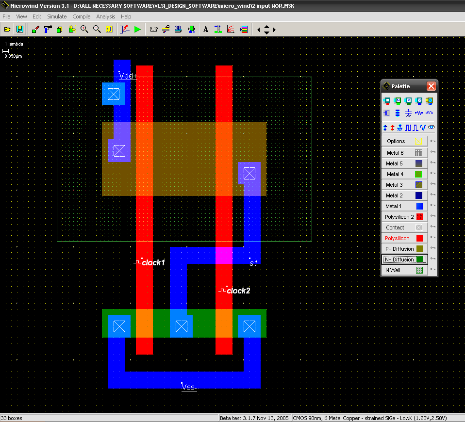
NOR Gate(2 input) layout | All For Students

Nor Gate - Custom IC SKILL - Cadence Technology Forums - Cadence Community

lab6

integrated circuit - NAND gate LVS problems in Cadence Virtuoso

Cadence tutorial - Layout of CMOS NOR gate - YouTube